Solved

Why is ZEMAX drawing the mirror substrate on the wrong side for a user-defined aperture?


ISHFM

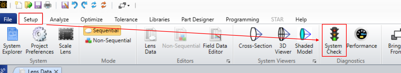
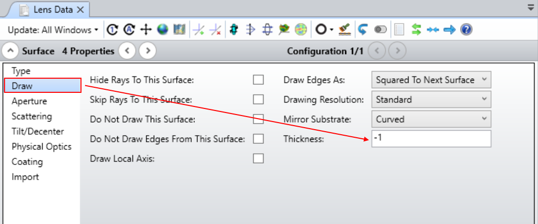
I’m working on a model for galvanometer mirrors that have a polygonal shape. For the mirror surface, when I set the aperture to the user-defined file (X,Y points clockwise, without a redundant endpoint), and draw the surface as a flat substrate with some thickness, the rays appear to travel through the substrate and reflect on the other side. 


I would like the mirror to be on the side that the rays see first. Is there a way to change that?

Best answer by MichaelH

Hi Ilya,

Can you run the System Check utility? 

If this shows 0 Warnings and 0 Errors, then I would simply make the substrate thickness a negative value.  

The Substrate Thickness is a non-optical value and only effects the display on a layout, but it has no effect on ray tracing (in fact, nothing in the Draw properties effects the ray trace, it only effects the layout plots).  So if there are no errors and you’re only concerned about the visual layout, just swap the signs of the substrate. 

View original
Did this topic help you find an answer to your question?

4 replies

Mike.Jones
En-Lightened
Forum|alt.badge.img+3
  • En-Lightened
  • 113 replies
  • May 6, 2023

Check the signs of your thicknesses coming at and leaving the mirror.  The thickness sign always reverses at a mirror.  If you have two negative or two positive thicknesses either side of a mirror, Zemax will just do what it is told, which in this case would be incorrect.


ISHFM
  • Author
  • Monochrome
  • 1 reply
  • May 7, 2023

Thanks for the reply. I did check to make sure that thicknesses are defined correctly. It appears that the rays are traced correctly when I have these galvanometer mirrors defined in a separate file, copied and pasted out of the master file I’m working on. Is there another potential solution given that there’s nothing wrong with the thicknesses?


Forum|alt.badge.img+2

Hi @ISHFM 

I would have guessed the same as @Mike.Jones to be fair. Can you fletch your rays to be sure everything is defined correctly? Also feel free to share your file here or on the support.


MichaelH
Ansys Staff
Forum|alt.badge.img+2
  • Ansys Staff
  • 342 replies
  • Answer
  • May 18, 2023

Hi Ilya,

Can you run the System Check utility? 

If this shows 0 Warnings and 0 Errors, then I would simply make the substrate thickness a negative value.  

The Substrate Thickness is a non-optical value and only effects the display on a layout, but it has no effect on ray tracing (in fact, nothing in the Draw properties effects the ray trace, it only effects the layout plots).  So if there are no errors and you’re only concerned about the visual layout, just swap the signs of the substrate. 


Reply


Cookie policy

We use cookies to enhance and personalize your experience. If you accept you agree to our full cookie policy. Learn more about our cookies.

 
Cookie settings