I need to perform some basic surface roughness analysis and would like to have an approximate reference point. In my case the surface roughness needs to be expressed as Ra value, arithmetic mean of the profile height deviations. What are typical surface roughness values expressed as Ra for “cheaper” Illumination grade optics ?
Is possible to get Ra ≤ 0.025 um in a cost-effective machining processing without post polishing steps ?
What is the simplest way to simulate surface roughness Ra (or RMS) quality in Zemax ?
marko
Page 1 / 1
I suggest you call or on-line chat with Edmund Optics to get the surface roughness spec for your lens of interest. Here’s a good app note that discusses polishing options (including values of surface roughness before and after superpolishing): Superpolished Optics
This is a generic statement from Edmund Optics about surface finish:
5 nm RMS is “typical quality,” but I don’t know what a value is for “cost-effective machining.” You could also try contacting Optimax.
Here’s a good paper that discusses modeling of surface scatter: Scatter Models for Stray Light Analysis. Specifically, it provides examples of ABg parameters for various RMS surface roughness values.
Hi Marko,
There is a knowledge base article on roughness simulation using the Rq parameter (for well polished surfaces). a an Rq are usually in the same order of magnitude
However, be aware that Ra (or even Rq or any set of additional roughness parameters, skewness, kurtosis, etc.) is not enough to “simulate” the effect of roughness in general, only within a set of assumptions (e.g. the roughness is mostly circular symmetric, very small, at a given frequency). It is useful to set acceptable limits of roughness once you can test your specific manufacturing and know that it is reproducible.
Hi Marko,
To complement Ray’s answer, for surface roughness analysis in OpticStudio, you can apply a scatter profile to the object in question. OpticStudio offers a variety of methods for modeling different scatter profiles that you can read about in What scattering models are available in OpticStudio? – Knowledgebase (zemax.com) or in the Help Files at “The Setup Tab > Editors Group (Setup Tab) > Non-Sequential Component Editor > Non-Sequential Overview > Scattering (non-sequential overview)”. The surface roughness can help to identify which scattering model would be appropriate, but a surface roughness doesn't give enough information on how the surface will scatter light. There is a useful discussion in this forum thread: Scattering analysis of transparent objects with VDI roughness surface finish.
Of particular help to you may be the surface scattering DLL called “K-correlation.DLL” which allows you to incorporate a surface roughness value, sigma (although sigma is defined as RMS so you’d have to convert from Ra). This can be found by selecting the object in question on your NSC Editor, opening its object properties, clicking on Coat/Scatter, choosing User Defined from the drop down menu next to “Scatter Model” and then selecting K-correlation.DLL from the drop down menu next to “DLL Name”. More information about how to model surface scattering using K-correlation can be found at How to model surface scattering via the K-correlation distribution – Knowledgebase (zemax.com).
OpticStudio also provides a tolerance operand that specifically targets surface irregularity: TEZI. If Standard or Even Asphere surfaces are used to describe the nominal system OpticStudio replaces them with Zernike Standard Sag surfaces for tolerancing. In sequential mode, we typically use the tolerancing operand TEZI to tolerance the RMS of the sag. It is well described in the Help System under The Tolerance Tab > Tolerancing Group > Tolerance Data Editor > Tolerance Operands > TEZI: Tolerance on Surface Irregularity Using the Standard Zernike Model. You can also read more information about TEZI here: How to use TEZI to tolerance for manufacturing-related surface sag error – Knowledgebase (zemax.com).
I hope this helps.
Best regards,
Moj
Hi Jeff,
thank you for the articles, I did some searching and found that typically RMS can range from 10 nm for low quality to 1 nm and below for higher quality optics. Optimax cost estimator docs also gives RMS range from 5 nm (commercial quality), 2 nm (precision quality) and 1 nm (lower bound for cost estimate).
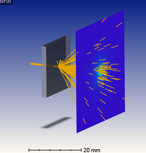
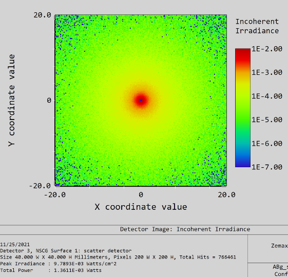
I made a simple test in Zemax to get some sense on the different RMS values. I have a glass plate and a rectangular beam 0.5mm x 0.5mm passing through the plate and hitting a detector. The beam is blocked just in front of the detector so I can better see the scattering effects from the last surface of the glass plate. The last surface of the glass plate has an ABg scattering model applied in transmission.
I have ABg scattering model as in the article: BK7, RMS 2 nm at 587.6 nm, A = 0.000161, B = 0.001 and g = 1.5. The fraction of initial beam power (1 W) scattered away due to the surface roughness is on the order of 1E-03 W, which seems a plausible result to me.
But if I try to calculate the parameter A as per in the article
s = 2 nm
dn = 1.5082 -1 = 0.5082
A = 3.50 (s dn/wl)^2 = 3.50 (2 nm] 0.5168/587.68nm] )^2 = 0.00001083
I don’t get the same parameter A. I would like to use this approximation for other RMS values, but I don’t know where is my mistake in calculating A.
@Ray, @Moj
thank you also on the info links, I have tried first to model RMS surface scatter as in the article linked by Jeff, this seems simple and good enough for first approximations. I will check other links later.
Marko
Hi Marko,
The example used in the article by Pfisterer is for *reflected* scatter from a glass surface (although the same ABg values could apply to any reflective surface with 2 nm RMS roughness -- but of course the absolute value for the total reflected power is governed by the Fresnel reflection coefficient). Your calculation for the A parameter looks correct for transmissive scatter. Also, if I’ve done the calculation correctly, the total integrated scatter (TIS) for your case, based on Eq. 2 in the article (with sigma = 2 nm, lambda = 588 nm, and dn = 0.5), is 1.1e-04. Hopefully your OpticStudio model with the new A value reports a similar result.