Dear Sir/Madam,
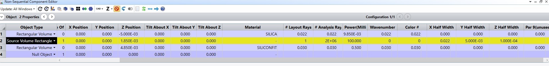
I am trying to create a new material which I named SILICONFIT in my design and use it as a silicon substrate. On top of the silicon substrate I put a rectangular volume named SIO2 made of SILICA. And inside the rectangular volume I put a source volume rectangle I named Light source. The dimension of them is stated below:
The lens units is Milimeters.
SIO2 (SILICA:) X1 half width: 0.022, Y1 half width: 0.022, Z length 0.00985, X2 half width:0.022, Y2 half width: 0.022
Source Volume Rectangle: Power: 100 (miliwatts), X half width 0.022, Y half width: 0.005, Z half width: 0.0001,
Silicon substrate: X1 half width: 0.03, Y1 half width: 0.03, Z length 0.5, X2 half width:0.03, Y2 half width: 0.03.
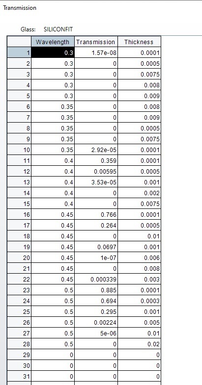
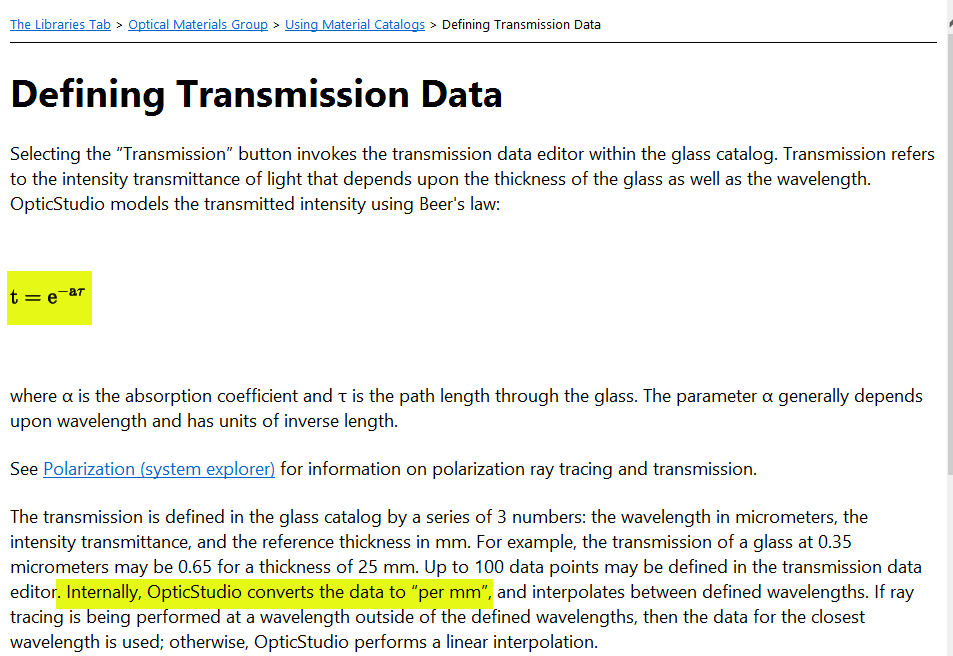
For the new material, I defined the transmission data followed the instruction in the user manual. Below is a screen capture of the transmission data I have defined.
The wavelength I used is 450nm with weight of 1.
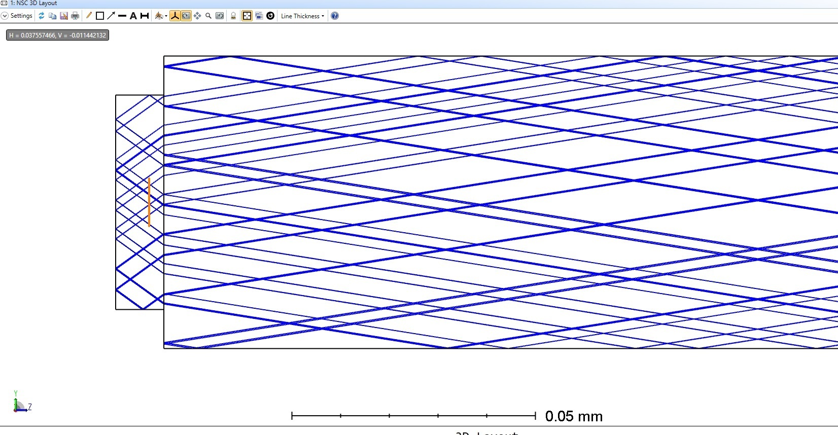
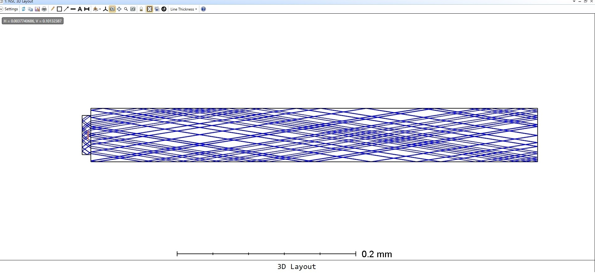
Based on the transmission data I put, after the light ray go through the substrate with a Z length of 0.5 which is 500 Micrometer, it should be absorbed with 0 intensity. But from the 3D layout, I noticed that a single light ray can be reflected many times inside the silicon substrate. In the picture below I have changed the layout rays to 1 to demonstrate the situation. I am not sure why this happen and please let me know if I have missed out any step or accidently did anything wrong.
Besides that, I noticed that once I remove the SIO2 rectangle volume, the light rays will terminate once they go through the Silicon substrate. That means, when I have the light source and the silicon substrate only, the light rays will terminate after they go through the silicon substrate once. They will never show multiple times of reflection inside the substrate.
Would really appreciate your help on this very confusing phenomenon I observed.
Waiting for your reply!
Best Regards,
Niu Jing