[Webinar] Designing Cell phone Camera Lenses with an Interoperability Workflow – Part 1 [Q&A]


Userlevel 6
Badge +2

This thread is dedicated to the upcoming webinar: Designing Cell phone Camera Lenses with an Interoperability Workflow – Part 1. Any questions received during the webinar will be responded to as a reply on this thread. Feel free to post your own questions! The speaker will be notified and will respond as long as the thread is still open.

Be sure to subscribe to this thread if you want to see additional discussion regarding this webinar topic. The thread will be open to new replies for a limited time following the event.


[The webinar has concluded]


Webinar details

Date: Tuesday, September 13th

Time: 6:00 - 6:45 AM PDT | 11:00 - 11:45 AM PDT

Presenter: Sandrine Auriol, Lead Application Engineer & Flurin Herrin, Application Engineer II

Abstract:

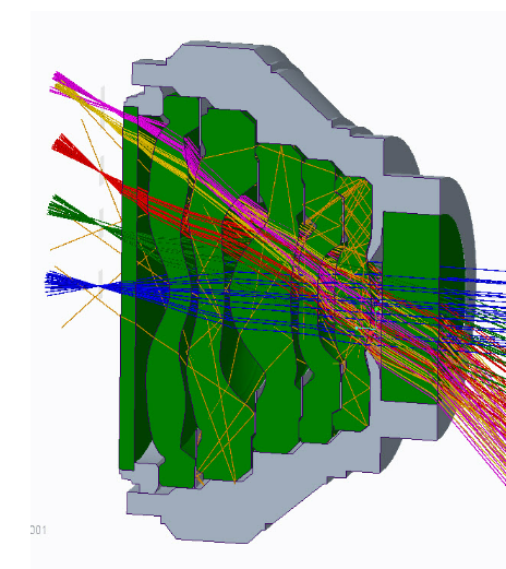
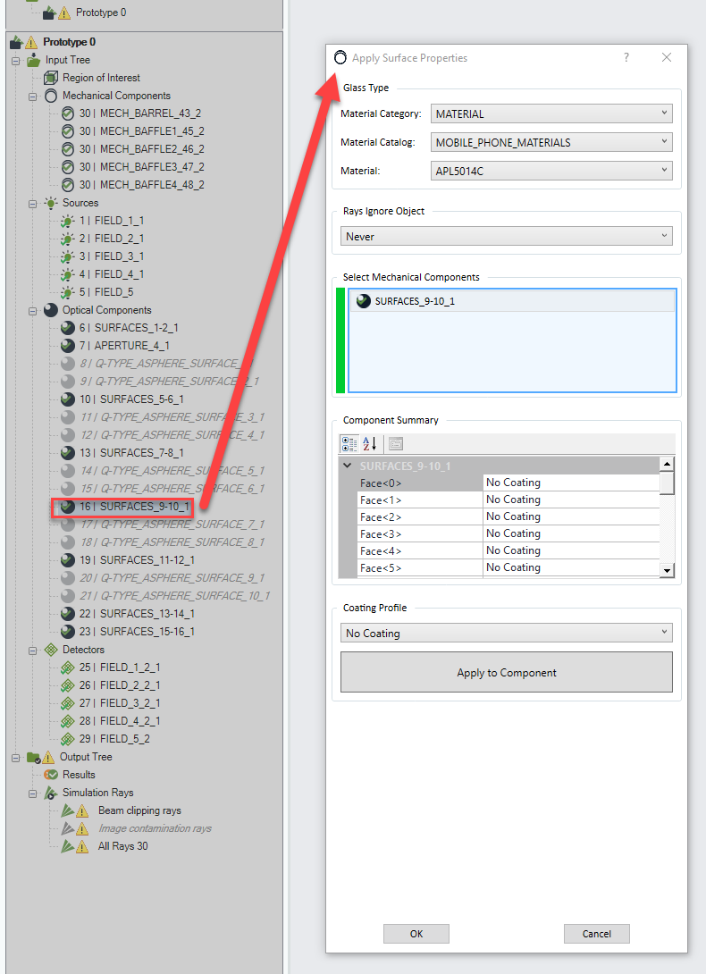
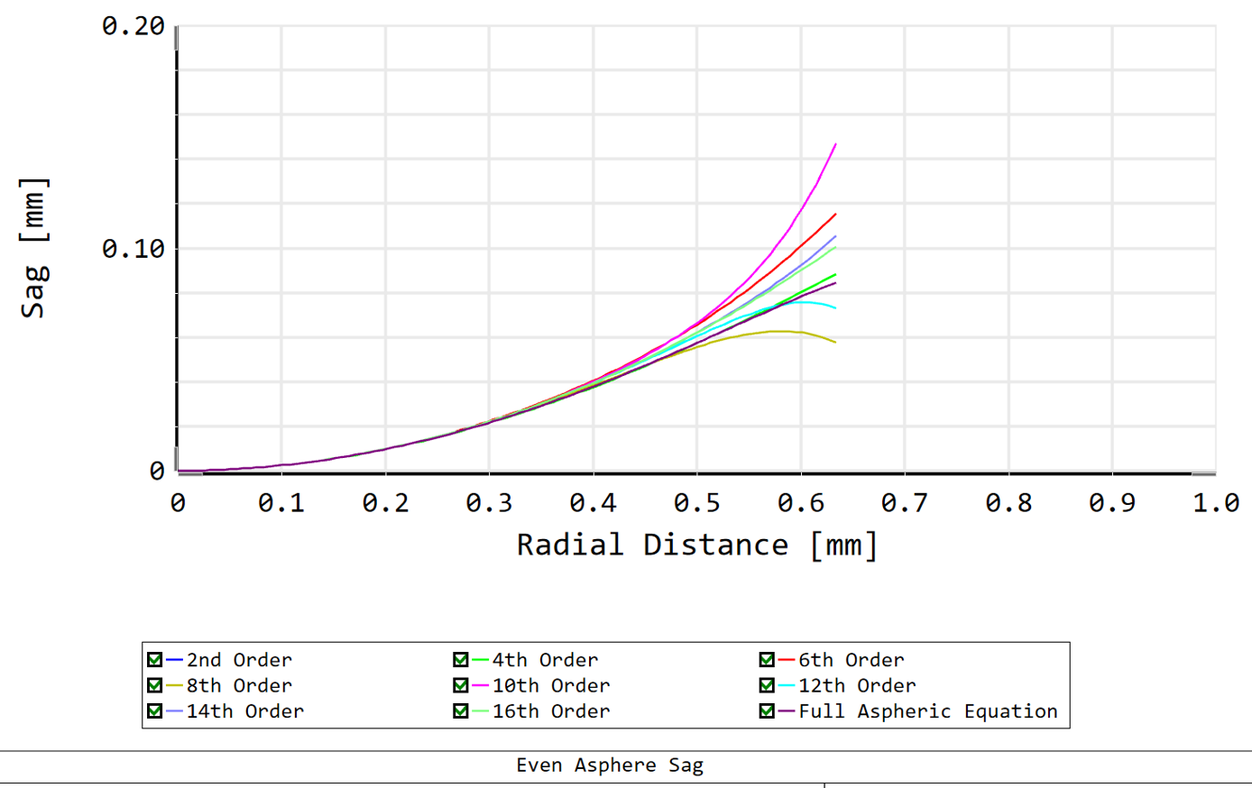
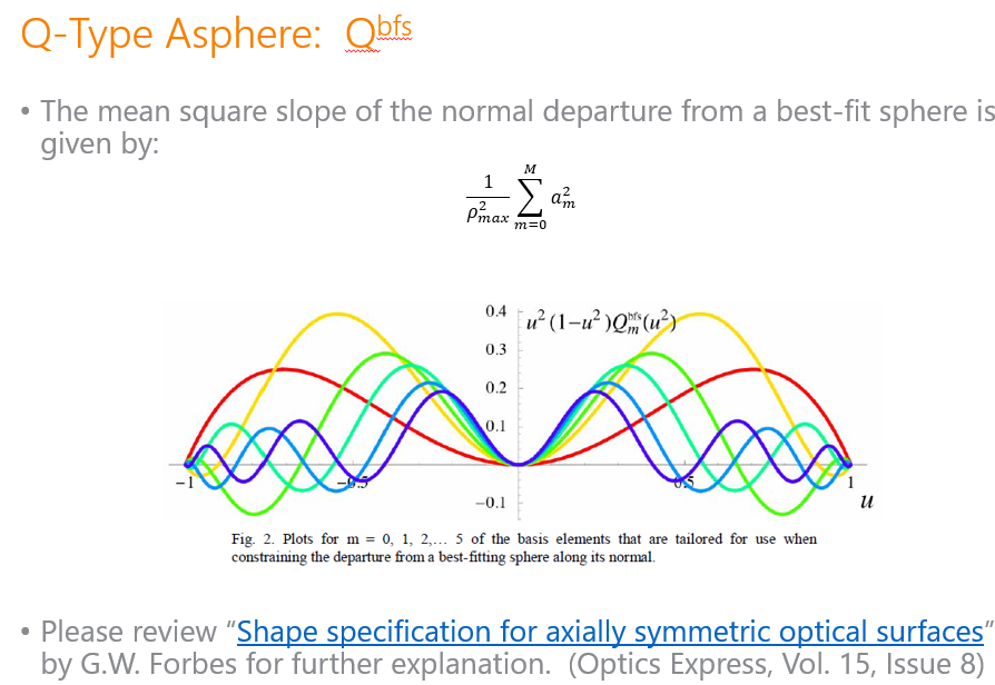
The cell phone market has experienced rapid growth over the past two decades. Cell phones improving significantly on a yearly basis, part of that evolution are also the camera lenses of the cell phones. With image quality reaching higher levels than ever, it also has become more important to have a more efficient and stable workflow to design such camera lenses. With the interoperability of the Ansys Zemax products, this design workflow can be applied in a highly efficient and dynamic way. In this first part of the Designing Cell phone Camera Lenses with an Interoperability workflow webinar series, Sandrine Auriol and Flurin Herren are presenting how to design the optical system of a Cell phone Camera lens from an Apple Inc. patent with Zemax OpticStudio using a Q-type Aphere surface approach and the Optomechanical Packaging with Zemax OpticsBuilder in Creo Parametric including the validation of the optical performance.

Allie 1 year ago

Watch the recording!

A recording of the webinar may be found here: Designing Cell phone Camera Lenses with an Interoperability Workflow – Part 1

View original

22 replies

Thanks for the presentation!
The optimization using the Q-Asphere type surface and then converting to the Even Asphere Surface Type was interesting. I have three related questions that popped up after the webinar:

  1. How large is the efficiency gain in the optimization (reduction in number of cycles, execution time...) when using the Q-Type Asphere vs. the Even Asphere Surface type?
  2. Is there a way to perform 1:1 conversion between Q-Type Asphere and Even Asphere surface type programmatically within a ZPL macro or using the ZOS-API?
  3. When Converting between the surface type, I could choose to allow change in the standard asphere part of the surface: Radius and Conic. Why does the conversion error increase when these options are selected?
Userlevel 1

Thanks for the webinar.


You talked about the material EP-10000 index 1.68. Do you know the Transmittance in the visible?

Also, do you know about vendors who fabircate asphere lenses with this material?


Thanks,

Nadav


Userlevel 6
Badge +2

Hi @simon.schroeder@zeiss.com!

  1. Zemax might optimize Even Aspheres better and faster, if we are simply looking at the convergence of the Merit Function. The Q-Type asphere surface is more computationally expensive, but in terms of shape the Q-type design result has more chances to be easier to manufacture and to test.
    I didn’t run a proper comparison though.
  2. For your 2nd question, yes there is. Please follow the link to G. W. Forbes’ paper https://opg.optica.org/oe/fulltext.cfm?uri=oe-15-8-5218&id=132268

(I don’t know if you have seen but we also have a thread where you might find some interesting posts)

  1. I suppose it is due to having unwanted degrees of freedom. But this is just a quick first thought.
Userlevel 6
Badge +2

Hi @nadav.amitai!

For material EP-10000 index 1.68, the best would be to contact Mitsubishi Gas Chemical Company, Inc, who is the manufacturer. We have a datasheet here but it says that the listed properties are portrayed as general information only and are not product specifications.

Here is the transmittance values that we have:

I don’t know vendors who fabricate with this material.

https://www.mgc.co.jp/eng/corporate/news/2019/launch-of-iupizeta-ep-10000-a-polycarbonate-resin-for-smartphone-camera-lenses-with-the-worlds-highe.html

Userlevel 6
Badge +2

Watch the recording!

A recording of the webinar may be found here: Designing Cell phone Camera Lenses with an Interoperability Workflow – Part 1

Userlevel 6
Badge +2

Q: Why the model built by the patent didn't yield the same characteristics (eg. MTF)?

A: It often happens that entering a model from a patent into a software gives slightly different results. I guess there can be different reasons for that. For example here, the materials are only defined by their index of refraction at d-light. The indexes of refraction, abbe numbers, asphere coefficients and thickness can have been rounded to a lower number of digits. There is no mention of the lenses diameters. All of that can lead to differences.

Userlevel 6
Badge +2

Q: What are the standard Manufacture tolerances (center, edge thickness, aspect ratio, decenter and tilt. etc)?

A: In the tolerance wizard in OpticStudio, you can find some default manufacture tolerances. The vendor can be selected as well as the Grade. One of the Grade option under the "Generic" vendor is Cell Phone Lens. In that case, the center thickness is +/-0.0015mm and the surface tilt is +/-0.05 degrees.


Userlevel 6
Badge +2

@Biswa RANJAN.Swain 

Q: What is the optimal setting for FFT MTF sampling etc to receive good corespondence of MTF?

A: The FFT MTF is based upon an FFT of the pupil data. So I believe that checking the sampling of the FFT PSF can be a good idea to check if the MTF sampling is enough. 

Userlevel 6
Badge +2

Q: Is the RI spike after 42,75 FOV something real that we would see if we build the optics? Why does it happen and how do we remove the spike?

A: We had some internal discussions about this spike that happens approximately at 45 degrees. A few things are going on in this design. The diameters were not given in the patent. To avoid "non-manufacturable" shape, we limited some diameters but that means that off-axis fields are vignetted. If we remove the apertures, we can see the RI going up at 47.5 degrees. I think both the 3D layout and the spot diagram are good indicators of the problem. The 3D layout shows rays departing from the bundle due to extreme sag in the asphere.

The RMS vs field (RMS spot radius) also shows the spike.

The spot radius gets larger for off axis field of view, but drops back at 47.5 degrees.

Maybe the rays that depart from the bundle are vignetted by the apertures for that field of view and that creates a smaller radius.
A designer wouldn't ignore that issue, and it would be down to the optical designer and also mechanical designer to work together to eliminate an unwanted ray bundle that causes a bump in the relative illumination. And this issue is especially important as the vignetted rays will reappear later in the design when we extend the edges.

Userlevel 6
Badge +2

@Daniel.Raguin 

Q: what should be the minimum MTF value for manufacturing the lenses? / What all the points I have to consider for manufacturing the lenses?

A: I think the minimum MTF at different frequencies / fields is something that would be agreed from the start in the specifications. I guess there would probably be some margin from the nominal values.
For manufacturing the lenses, it is important to check that the design can be manufactured. I mentioned a couple of operands during the webinar. Then tolerancing this system will help get an understanding of the yield you could achieve with that kind of system.

Userlevel 6
Badge +2

Q: Could you explain what tolerance bands are used in cell phone design? how to execute Tolerance analysis?

A: Sure. For the tolerance bands, a starting point can be the tolerance wizard in OpticStudio as it contains default manufacture tolerances. The vendor can be selected as well as the Grade. One of the Grade option under the "Generic" vendor is Cell Phone Lens. 
Then another important point is the mechanical mounting of the lens. The lenses are stacked.


So a tilt in one lens will impact all the other lenses. I think that I would add manually the coordinate breaks to my lens system to mimic that behaviour. Then the multi-configuration editor can be used to check that the file has been set up properly. One configuration can be the nominal configuration and the 2nd one the toleranced one. Checking the behaviour of one configuration vs the other will help validate the model. 

Userlevel 6
Badge +2

Q: Hello, Is there a preferential glass catalog to be up to date with the latest mobile phone glass in use ?

A: The mobile phone lens comes with its own private material catalog. So far it is not part of the catalogs that come with the installation of the software.

Badge +3

@Andrew.Kadis 

Q: Are you able to perform parametric studies of size and location tolerances within Opticsbuilder?

A: A tolerancing function, much like the one in Zemax Optic Studio is in planning, so once all the tolerance operands and compensators have been defined, the tolerance analysis may be performed. Unfortunately I cannot give out an exact release date for this feature yet yet. 

Badge +3

Q: Is this design available in the student version? / Are the additional tools such as OpticsBuilder, Ansys and other tools available to install in the student version as well? / is it possible to get a copy of the slides for this webinar? Thank you! / The Image simulation feature is a fantastic feature in the OpticStudio. It would be really useful for my research project! Are there any additional tutorials on this? Thanks! / is tolerance one of the optical performance parameter measurements in OpticStudio/Creo OpticsBuilder? / is it possible to apply the optical design on various public datasets?

A: List,

Userlevel 6
Badge +2

@richard.berglind_01 

Q: Is it common for the STOP to be at the front of the optical design for smartphone lenses or can it be further inside the design?

A: I checked with my colleague @Chenfeng.Gu about this question. 
Commonly, cameras with a not too large full FOV (for example <100 degrees) have the STOP defined before the first surface. This considers the optical performance, package size and outward appearance. For wide-angle camera (with a bigger F# like 2.0/2.2 and a smaller aperture size), the STOP is defined within the lens.
One interesting thing to do is to look at your cellphone's camera lenses. By looking at them, you can easily find out which one is wide angle and which one is not. The STOP position will result in a different appearance.

So to summarize, the STOP position in a cellphone lens system is determined by optical performances, package size and outward appearance.

Userlevel 6
Badge +2

@Elisabeth.Karl

Q: For definition of a Q-type-Asphere manufacturable surface sag, which dimensions (values and tolerances) are common at most manufacturers for injection molding and slope / curvature / sag data?

A: I checked with my colleague @Chenfeng.Gu about this question. 
Q-type aspheres are not different than any aspheres, During the design phase, the Q-type asphere coefficients are optimized and then toleranced. Then before giving the lens drawing to the mould tooling department, the Q-type coefficients are converted back to even-asphere coefficients. Those even-asphere coefficients are the ones used by the manufacturing department. So the slope/curvature/sag data constraints are the same as any aspheres.

Userlevel 6
Badge +2

Q: I would like to ask regarding to IR filter component. Why did not you use the cover window's back surface for IR filtering. You would decrease one component...

A: I checked with my colleague @Chenfeng.Gu about this question. 
It is now common to use a blue glass to act as the IR cut filter in camera lens and then do coatings on the front and back sides of the filter to get the wanted wavelength pass.
For more information, have a look at this reference: 
https://spie.org/Publications/Proceedings/Paper/10.1117/12.981161?SSO=1


Badge +3

 @Andrew.Dennington 

Q: How do you tolerance all the aspheres so that you create the drawings for each lens

A: In OpticStudio the tolerancing option for extended Aspheres are limited, as an example is the TEZI operand not available. A workaround here could be a new campsite surface or otherwise you can apply a tolerance operand to the coefficients and check with a macro the amount which got added.

What you could also do in this Situation, is to look into the Drawing Option of Optics Builder. However the tolerancing options are also limited there.

Badge +3

Q: What did you change exactly at the STOP in OpticsBuilder to improve?

A: The optical STOP which has been added by Sandrine when she designed the optical system needs to be backed up by the Mechanical STOP, as this is a physically barrier for the light. To do so I have desgined the Barrel (Housing Mount) with a mechanical aperture in the front. This Aperture had a specific diameter, which was too small. Hence we had some Beam clipping. So what I have done is increase the diameter of the mechanical aperture on the Barrel component, with the Creo Native Sketch tool.  Shown on the image below


Badge +3

Q: For mechanical optimization, is it manually done? Is there also something like Merit function in Creo? / How to run ray trace in Creo?

A:  At the moment the mechanical “optimization” needs to be done manually yes. The way I usually approach it is to have some sort of first iteration of the mechanical part (May that be from a patent or an initial sketch), add this part to the optical components and then optimize manually it with the information gained from various ray traces. However, a similar feature as the Merit Function in OpticStudio is in planning for OpticsBuilder, this will very likely be build on top of the tolerancing features.

On the Ray Trace itself in Creo: This is one of the biggest advantages of OpticsBuilder, with the OB add-in you can actually run ray traces inside the Creo environment. An as the mechanical components are taken into account for the ray trace, you can see the influence of the mechanical components on the optical performance while you are designing them. 

Badge +3

@Sunny 

Q: How is image contamination calculated with opticsbuilder? Does it allow users to set surface properties freely?

A: When traced rays in the OpticsBuilder modified configuration take unintended paths to a detector, they contribute to image contamination. An unintended path is any path that did not exist in the OpticsBuilder baseline configuration ray trace. The percentage of image contamination rays is defined by the flux on an unintended path in the OpticsBuilder modified configuration divided by the flux on the OpticsBuilder baseline configuration multiplied by 100. If no mechanical components exist in the OpticsBuilder model the OpticStudio and OpticsBuilder baseline configuration results are used to calculate image contamination. So the formula would be:

On the Surface Properties: Yes the default surface property applied to mechanical geometry in OpticsBuilder is Black Anodized, which applies to imported parts and new parts created in Creo. 

If you want to change a mechanical part surface property use the Apply Surface Properties tool. The following scatter profiles are available for use:

  • MIRROR (95% reflectance)
  • Black Anodized
  • Black Foil 1% Reflectance Visible
  • Black Foil 2% Reflectance UV
  • Black Paint 1% Reflectance Visible
  • Black Paint 2% Reflectance UV
  • Black Paint 2% Reflectance Visible
  • Gold Anodized
  • Grey Anodized
  • Grey Plastic
  • Powdered Black Steel Post
  • Stainless Steel

For the optical components, we have nearly all the possibilities of the OpticStudio surface parameters range. So we can change the Material, we can add Coatings or apply Scattering Properties to a surface.


Userlevel 6
Badge +2

@Sheldon.Schwartz 

Q: The OpticStudio conversion from Q-Forbes to even asphere was said to be exact. Given this, why would a Q-Forbes converge to a solution where the even asphere would not. BTW, I have seen this same result. Thank you!

A: The conversion is exact yes. But in terms of optimization it is different because the software is only allowed to change the coefficients of each term. So it means that when the software is going to try to change a coefficient to evaluate the change in the merit function. In one case it will happen on a strictly 4th order, 6th order term while in the other case it will happen on a combination of 4th, 6th order terms. The combination of terms is done in a way that the coefficients have roughly the same amplitude and can be optimized together (they are orthogonal) while not cancelling (too much) each other.

I think it can be understood by looking visually at those terms. During the webinar, I showed a representation of these terms:


In terms of optimization and numerical accuracy, that will create a difference. This article explains it too: https://opg.optica.org/oe/fulltext.cfm?uri=oe-15-8-5218&id=132268

Reply